Practical EMC Design Optimization for Power Modules with Low EMI
Discover practical EMC design and optimization techniques for power modules to reduce EMI, improve PCB layouts, and ensure compliance efficiently.
If you’re designing with semiconductor power modules like IGBTs, MOSFETs, or the latest SiC/GaN devices, you know that managing EMC is more than just a checkbox—it’s a critical step to ensure low EMI and rock-solid performance. High-speed switching brings unavoidable noise challenges: conducted and radiated emissions can throw off your entire system if left unchecked.
In this post, I’m peeling back the curtain on practical EMC design and optimization for power modules—no fluff, just proven strategies to pinpoint noise sources, optimize PCB layouts, pick the right filters, and navigate compliance smoothly. Whether you’re tackling common-mode noise, layout parasitics, or tricky trade-offs between efficiency and emissions, the insights here will help you hit first-pass EMC success quickly and cost-effectively.
Ready to cut through the complexity and get hands-on with your next power electronics design? Let’s dive into the essentials that make your modules perform cleaner, quieter, and more reliably in the real world.
Understanding EMC Fundamentals in Power Modules
When designing power modules, understanding EMC (Electromagnetic Compatibility) fundamentals is crucial to ensure reliable operation and compliance with standards. Engineers often ask, “How do I control emissions and improve immunity without sacrificing performance?” The key to answering that lies in grasping core EMC concepts and recognizing the unique challenges power modules present compared to discrete designs.

Key EMC Concepts in Power Modules
- Conducted Emissions (CE): Noise traveling along power lines can interfere with nearby equipment. Managing these emissions prevents regulatory failures.
- Radiated Emissions (RE): Electromagnetic fields radiate from the module, potentially causing electromagnetic interference (EMI) issues in the surrounding environment.
- Immunity (ESD, Surge, EFT): Power modules must withstand electrostatic discharges, voltage surges, and electrical fast transients to ensure system robustness.
- Susceptibility: The module’s vulnerability to external electromagnetic disturbances must be minimized to maintain system operation under EMI-rich conditions.
Primary Noise Sources in Power Modules
The main culprits behind EMI in power modules are:
- High dv/dt and di/dt from switching devices: Rapid voltage and current transitions generate significant broadband noise.
- Switching Devices: IGBTs, MOSFETs, and other switches produce high-frequency noise during on/off cycles.
- Currents in different modes: Common-mode currents (flows with respect to ground) and differential-mode currents (between power lines) require separate mitigation approaches.
- Parasitic Elements: Stray inductances, capacitances, and mutual couplings within the module and PCB contribute to unexpected resonances and emissions.
Standards and Test Methods
Compliance hinges on standardized testing like CISPR 11/25 and the IEC 61000 series, which specify limits and testing procedures for power electronics. These standards help identify pass/fail conditions early, preventing costly redesigns later.

Unique EMC Considerations in Power Modules
Unlike discrete components, power modules bring specific challenges:
- Integrated Packaging: Internal parasitics are harder to control, requiring careful packaging and layout.
- Thermal Coupling: Heat spreaders and heatsinks can affect parasitic capacitance and inductance, influencing emissions and immunity.
- Compact Design: The dense packing of high-current paths and internal components increases the risk of resonances and parasitic coupling.
Mastering EMC fundamentals tailored to power modules enables you to proactively address EMI issues, ensuring your designs meet standards while optimizing performance and reliability.
Identifying and Analyzing EMI Sources in Power Modules
Switching behavior is often the main culprit behind EMI issues in power modules. Variables like gate drive parameters, dead time, and slew rate directly influence noise generation. Fast switching turns high dv/dt and di/dt into sources of electromagnetic interference, making careful gate drive control essential. Adjusting the gate drive slew rate can significantly reduce switching noise, or consider active methods like spread-spectrum modulation to shape the noise spectrum.
Parasitic effects also play a big role in EMI. Stray inductance in busbars and module packaging creates unwanted voltage spikes, while inter-winding capacitance in magnetic components can couple noise into sensitive circuits. Additionally, coupling between the power module and heatsinks can contribute to radiated emissions. Managing these parasitics involves optimizing busbar layout, using low-inductance wiring, and proper shielding.
Common failure modes related to EMI include excessive common-mode noise caused by parasitic capacitance to ground—something that can often be mitigated with better grounding strategies. Differential-mode ripple, from input and output currents, may lead to EMI compliance issues, especially in high-current designs. Resonances within the module or layout can amplify emissions, so it’s crucial to identify these resonant frequencies early.
To locate and analyze these EMI sources, several diagnostic techniques are used. Near-field probing helps visualize local electromagnetic fields around the power module. Line-input/line-output (LISN) measurements provide standardized conducted emissions data, while time-domain analysis reveals transient switching noise. Frequency-domain analysis assists in pinpointing specific resonances or parasitic coupling paths, making it easier to implement targeted fixes.
For effective EMI mitigation, understanding these root causes and applying the right measurement techniques are key steps on the path to compliance, especially when designing advanced power modules like those seen in high-performance inverter systems or electric vehicle powertrains.
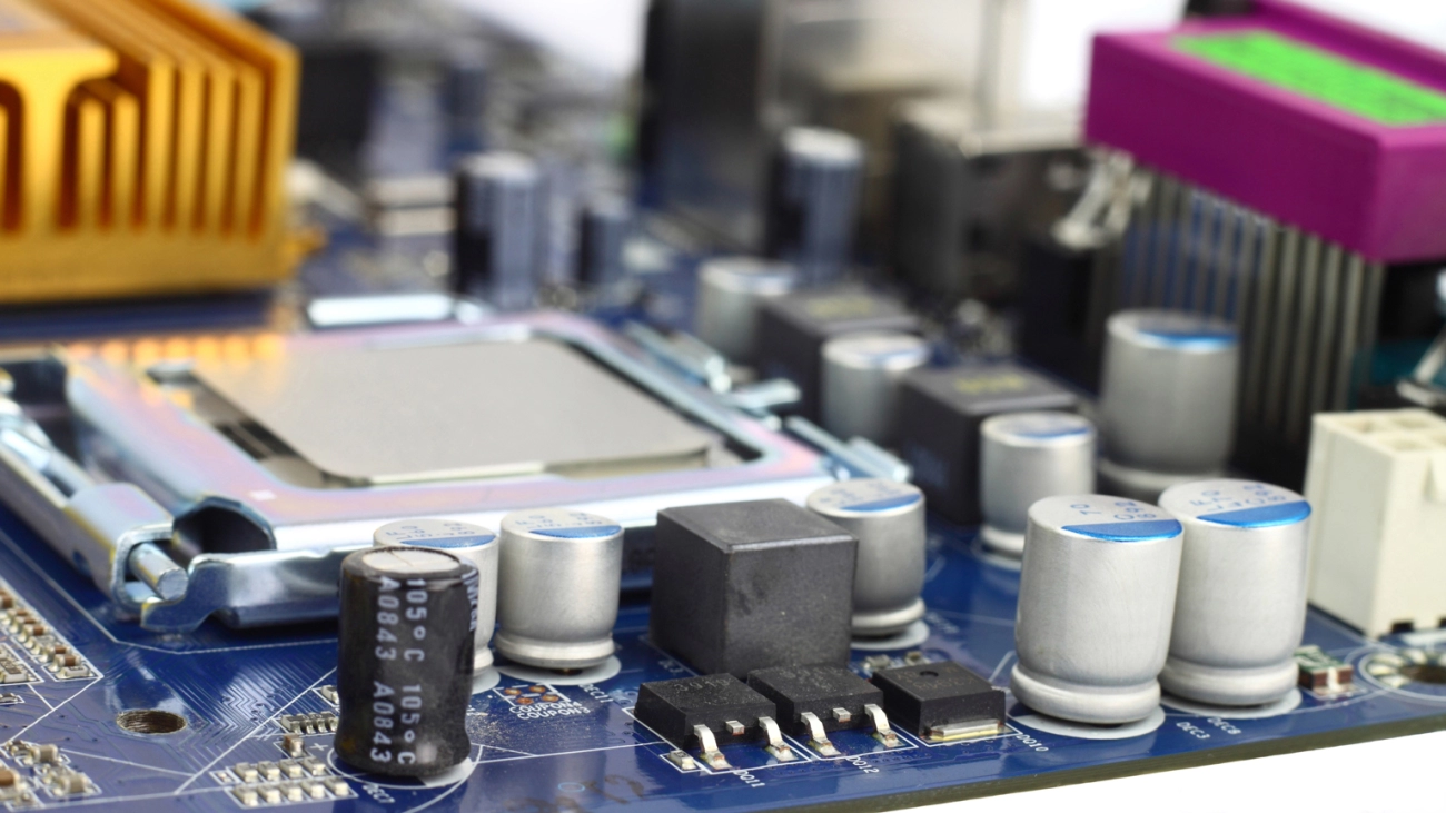
Practical PCB Layout Optimization Techniques for Power Modules and EMI Reduction
Optimizing your PCB layout is crucial for practical EMC design and minimizing EMI in power modules. Here’s how to get started:
Minimize Loop Areas to Reduce Noise
Large loop areas can act like antennas, radiating unwanted emissions. Focus on:
- Power commutation loops: Keep the switching loop, which includes the drain/source and the power return path, as small as possible.
- Gate drive loops: Shorten the gate loop to limit high dv/dt noise coupling.
- Return paths: Ensure a clear, low-impedance return route for currents, especially for high-frequency switching.

Grounding Strategies for EMI Control
Effective grounding helps suppress common-mode currents and noise:
- Solid reference planes: Use continuous ground planes to provide low-impedance paths and reduce parasitic inductance.
- Star grounding vs. multi-point: For power modules, star grounding can help avoid ground loops, while multi-point grounding may be suitable where parasitic effects are controlled.
- Low-impedance paths: Establish direct, low-inductance connections from heatsinks, busbars, and module grounds to minimize parasitic effects and parasitic capacitance to ground.
Component Placement and Partitioning
Good component layout prevents noisy signals from affecting sensitive circuits:
- Separate noisy power sections (like switches and high-current paths) from control and measurement circuits.
- Strategic placement of decoupling capacitors: Position these close to the power pins to effectively filter high-frequency switching noise.
Layer Stack-up Best Practices
Proper PCB layer design supports EMI mitigation:
- Use dedicated reference (ground) planes for signal integrity and shielding.
- Follow 3W/20H rules (for via and trace widths/heights) to optimize high-frequency current paths.
- Via placement and optimization: Use multiple small vias instead of fewer large vias to reduce parasitic inductance in high-frequency currents.
Power Module Integration Tips
When integrating power modules like HiRel IGBTs or SiC modules, taking special care can significantly improve EMC performance:
- Busbar design: Keep busbars short and wide to reduce parasitic inductance.
- Heatsink grounding: Ensure proper bonding and grounding of the heatsink to prevent radiated fields.
- Shielding considerations: Use metal enclosures or shields around the module to contain radiated emissions and prevent external interference.
Implementing these PCB layout techniques can help meet EMC standards and optimize power module performance, especially in high-current industrial applications. For advanced busbar and grounding tips, check out HiSilicon’s power modules for their specific integration recommendations, including shielding strategies to suppress radiated fields.
Filter Design and Component Selection for EMI Suppression
Choosing the right filters and components is key to reducing EMI in power modules. There are two main types you’ll want to consider: differential-mode and common-mode filters. Common topologies include LC, π, T configurations, and hybrid approaches that combine these for better performance.
Practical component choices
- X/Y capacitors: Excellent for blocking high-frequency EMI on power lines, with X capacitors across lines and Y capacitors to ground.
- Common-mode chokes: Help suppress noise that appears equally on both lines, reducing radiated emissions.
- Ferrite beads: Useful for high-frequency attenuation without adding too much parasitic inductance.
- Nanocrystalline materials: These high-performance cores are great for minimizing core losses and saturation, especially in high-frequency environments.
Parasitic-aware design considerations
- Account for ESL (Equivalent Series Inductance) and ESR (Equivalent Series Resistance) in capacitors to avoid resonances.
- Consider core losses and saturation for inductors to prevent unwanted resonance or increased heat under load.
Optimization techniques
- Follow a measure-simulate-iterate cycle:
- Measure how your filter performs.
- Use simulation tools for design validation.
- Adjust components to meet your EMI goals without over-sizing, which impacts efficiency and cost.

Integration with power modules
- Proper placement of input/output filters is vital—position them close to the power module to maximize effectiveness.
- Use filters to damp resonances and leverage internal module optimizations, like built-in shielding or filtering features, to minimize radiated noise.
For more on selecting the right power modules and their EMI considerations, check out HiRel Power Modules. It’s all about combining smart component choices with good design practice to keep EMI under control without sacrificing size or efficiency.
Advanced Optimization Strategies and Trade-Offs in Practical EMC Design for Power Modules
When designing power modules with optimal EMC performance, advanced strategies involve a mix of simulation, innovative gate drive methods, and smart material choices—all aimed at balancing EMI reduction with other key performance factors like switching losses and power density.
Simulation-Driven Design for Accurate Prediction
Using tools like SPICE, finite-element analysis, or specialized EMC simulators helps predict potential EMI issues before laying out the physical design. These models allow us to test various layouts and component choices virtually, saving time and reducing costly iterations. Pre-layout simulation ensures that the power modules meet EMC standards and minimizes the risk of costly redesigns later.
Gate Drive Techniques to Minimize Switching Noise
Adjustable slew rates are a simple yet effective way to reduce dv/dt and di/dt noise, lowering conducted emissions and radiated fields. Active Miller clamping helps control switching transients, preventing excessive voltage overshoot and ringing. Spread-spectrum modulation distributes switching noise over a wider frequency range, making EMI more compliant with standards like CISPR 11/25. These techniques are essential for maintaining high power density while controlling EMI.
Material and Packaging Choices for EMC Improvements
Selecting low-inductance modules, such as those in HiRel power modules, can significantly cut parasitic inductances that cause high-frequency noise. Advanced substrates and innovative packaging designs, which incorporate thermal-EMC co-design, provide multiple benefits—cooling efficiency and electromagnetic compatibility. These approaches help keep parasitic effects in check and improve overall EMI performance.
Balancing Objectives: Reducing EMI vs. Power Loss and Cost
Achieving EMC goals shouldn’t come at the expense of efficiency or cost. Practical iterative improvements involve fine-tuning layouts, optimizing component selection, and employing filtering strategies. For example, controlled switching transitions can lower EMI while maintaining power density. These real-world trade-offs mean manufacturers can design power modules that comply with standards without overly increasing size or reducing performance.
Emerging Approaches: Soft Switching, Wide Bandgap Devices, and Active Filters
Innovative methods like soft-switching topologies help minimize switching losses and EMI simultaneously. Wide-bandgap devices such as SiC and GaN (see our blog on wide-bandgap technology) inherently generate less EMI due to faster switching and lower switching energy. When combined with active filtering techniques, these approaches push the boundaries of practical EMC optimization—making power modules more robust and compliant in demanding applications.
Balancing these advanced strategies allows us to meet strict EMC standards while still pushing for better efficiency and higher power density. It’s about making informed choices and applying the right combination of simulation, material, and design techniques to stay ahead in a competitive market.
Testing, Troubleshooting, and Compliance Pathways for Power Modules
When it comes to ensuring your power modules meet EMC standards, understanding the difference between pre-compliance testing and full certification is key. Pre-compliance offers a cost-effective way to catch EMI issues early. It usually involves setting up simple tests with basic equipment like LISNs and portable analyzers. Full certification, however, requires formal testing in certified labs, which can be more expensive but ensures your product passes standards like CISPR 11/25 and IEC 61000 series.
Troubleshooting power module EMC problems step-by-step can save time and money. First, start by separating common mode (CM) and differential mode (DM) noise sources. Using near-field probes and spectrum analyzers helps identify hotspots—those problem areas that generate excessive EMI. Once pinpointed, targeted fixes such as improving grounding, adding filters, or redesigning layout sections can significantly reduce emissions.
Avoid common pitfalls that lead to EMI failures. Simple quick wins include enhancing cable shielding and termination, ensuring proper enclosure bonding, and revising PCB layouts to reduce parasitic inductances. For example, low-inductance busbar design and strategic component placement are crucial in minimizing high dv/dt noise and parasitic effects. These small but impactful adjustments often yield major improvements in EMC performance.
Accurate documentation and reporting are essential for certification. Collect comprehensive measurement data—covering both conducted and radiated emissions—and demonstrate margins against the limits. Clear records help in troubleshooting and provide a solid case during compliance submissions. By following a systematic approach, you can effectively manage the EMC testing process and get your power modules certified faster, avoiding costly delays or redesigns.
If you’re working with advanced power modules like HIITIO’s 1200V IGBT power modules, understanding these EMC pathways ensures your design not only performs well but also passes compliance smoothly.
Case Studies and Real-World Applications of Practical EMC Design in Power Modules
In real-world applications, effective EMC optimization truly makes a difference. For example, in industrial motor drives, we reduced the size of the filters significantly while still meeting CISPR emission limits. This not only saved space but also improved overall efficiency and reliability. By applying practical EMC design techniques, such as minimizing parasitic inductance and optimizing grounding, we can achieve these kinds of impressive results.
In the realm of EV and renewable energy power conversion, dealing with high-voltage challenges and the specifics of wide bandgap devices like SiC and GaN is critical. Our power modules incorporate advanced packaging, like the HIITIO 1200V Easy-3B IGBT power module, which helps control switching noise and suppress EMI emissions. This makes high-voltage systems more manageable from an EMC perspective.
Our power modules specifically leverage built-in EMC advantages through innovative packaging and characterization. This internal optimization, combined with thoughtful PCB layout and filtering strategies, helps reduce radiated and conducted emissions at the source, saving customers from costly troubleshooting or compliance issues.
Finally, the before-and-after spectra illustrate how design iterations and targeted measures lead to quantifiable improvements. Reduced EMI levels, lower filter sizes, and shorter development cycles all translate to cost, size, and time savings. These case studies show the true value of applying practical EMC design and optimization techniques, especially with robust modules like HIITIO’s offerings that integrate advanced packaging to simplify compliance.


