Why SiC Power Modules Are Replacing Silicon: A Technical Deep Dive
Silicon Carbide (SiC) power modules are revolutionizing electric vehicle drivetrains, data centers, and renewable energy systems with 2-5% efficiency gains and 3x higher power density compared to traditional silicon IGBTs.
With the rapid development of power electronics technology, Silicon Carbide (SiC) semiconductor power modules are gradually replacing traditional silicon-based power modules, becoming the preferred solution for high-performance power conversion systems.
As a representative of third-generation semiconductor materials, SiC demonstrates tremendous application potential in electric vehicles, photovoltaic inverters, industrial drives, and data center power supplies, thanks to its superior physical properties.
This article provides an in-depth analysis of the technical advantages of SiC power modules compared to traditional silicon-based modules from multiple dimensions, including material characteristics, device performance, loss mechanisms, and system efficiency, ultimately providing selection guidance for engineering applications.
I. Material and Device Key Performance Indicators Comparison
1.1 Fundamental Material Property Differences
SiC and Si exhibit fundamental differences in physical properties, which determine the performance limits of devices. In terms of bandgap width, SiC measures approximately 3.26 eV, while Si is only 1.12 eV. This nearly threefold difference enables SiC devices to withstand higher operating temperatures and electric field intensities. Regarding the critical breakdown electric field strength, SiC reaches 2.5-3.0 MV/cm, nearly 10 times that of Si (0.3 MV/cm). This means that for the same voltage rating, the drift region thickness of SiC devices can be significantly reduced, thereby substantially lowering the on-resistance.
| Parameter | Silicon (Si) | Silicon Carbide (4H-SiC) | Engineering Implication |
|---|---|---|---|
| Bandgap Energy (Eg) | 1.12 eV | 3.26 eV | Lower leakage current and better high-temperature stability |
| Critical Breakdown Electric Field | ~0.3 MV/cm | ~2.5–3.0 MV/cm | Thinner drift layer for the same voltage rating |
| Thermal Conductivity | ~1.5 W/cm·K | ~4.5–4.9 W/cm·K | More efficient heat dissipation |
| Maximum Junction Temperature (Device Level) | 150 °C | 175–200 °C | Simplified thermal management |
| Intrinsic Carrier Concentration | High | Extremely low | Superior stability at elevated temperatures |
Thermal conductivity is a critical parameter affecting the heat dissipation performance of power devices. SiC’s thermal conductivity is 4.9 W/(cm·K), approximately 3.3 times that of Si (1.5 W/(cm·K)). Higher thermal conductivity enables SiC devices to more effectively conduct heat away during high power density operation, reducing heat accumulation. In terms of saturated electron drift velocity, SiC achieves 2.0×10^7 cm/s, twice that of Si (1.0×10^7 cm/s). This advantage directly translates into faster switching speeds and lower switching losses.
1.2 Device-Level Key Parameter Comparison
At the actual device level, SiC MOSFETs demonstrate superior performance compared to silicon-based IGBTs across multiple core indicators. Regarding on-resistance (Rds(on)), taking the 1200V voltage rating as an example, SiC MOSFETs can achieve specific on-resistance as low as 1-3 mΩ·cm², while the equivalent resistance corresponding to the saturation voltage drop of the same-rated Si IGBTs typically ranges from 5-10 mΩ·cm². This means that during high current operation, SiC devices exhibit lower conduction losses.
The differences in switching characteristics are even more pronounced. SiC MOSFETs, as majority carrier devices, do not suffer from minority carrier storage effects, with switching times typically in the 20-50 ns range, whereas silicon IGBTs require 100-300 ns due to the need to handle minority carrier extraction processes. Faster switching speeds not only reduce switching losses but also enable systems to operate at higher switching frequencies, thereby reducing the volume and weight of passive components (such as inductors and capacitors).
Junction temperature capability is an important indicator of power device reliability. SiC devices can achieve maximum junction temperatures of 175-200°C, with some high-temperature designs reaching up to 250°C, while traditional silicon-based IGBTs are typically limited to 150-175°C. Higher junction temperature margins mean that under the same cooling conditions, SiC systems can deliver greater power output, or under the same power conditions, can simplify thermal design, reducing system cost and volume.
| Parameter | Si IGBT | High-Voltage Si MOSFET | SiC MOSFET |
|---|---|---|---|
| Typical Voltage Rating | 1200 V | 600–900 V | 650–1700 V |
| Conduction Characteristic | VCE(sat) | High RDS(on) | Significantly lower RDS(on) |
| Reverse Recovery Behavior | Severe | Noticeable | Nearly negligible |
| Switching Speed | Slow | Moderate | Fast (nanosecond range) |
| Recommended Switching Frequency | < 20 kHz | < 50 kHz | 50–300 kHz |
| High-Temperature Performance | Moderate | Moderate | Excellent |
| Overall Power Loss | High | Medium | Low |
II. Device-Level Performance Comparison Analysis
2.1 Static Characteristic Comparison
In static operating states, conduction loss is the primary source of energy consumption. The conduction characteristics of SiC MOSFETs exhibit approximately linear resistive behavior, with Rds(on) increasing with temperature, having a temperature coefficient of about 0.6-0.8%/°C. In contrast, the saturation voltage drop Vce(sat) of silicon IGBTs includes both a fixed threshold voltage component and a resistive component, with positive temperature coefficient characteristics causing conduction losses to increase more significantly at high temperatures.
Taking 100A operating current as an example, a 1200V SiC MOSFET (Rds(on)=10mΩ) has conduction losses of approximately 100W, while a same-rated silicon IGBT (Vce(sat)=2V) has conduction losses of about 200W. Under light load conditions, the advantage of SiC devices becomes even more apparent, as the fixed threshold voltage portion of IGBTs accounts for a higher proportion at low currents. Additionally, the reverse conduction characteristics of SiC MOSFETs allow their body diodes to be used for freewheeling, eliminating the need for external freewheeling diodes and simplifying circuit topology.
2.2 Dynamic Characteristic Comparison
The switching process represents the most significant performance difference among power devices. The turn-on and turn-off processes of SiC MOSFETs are controlled by gate charge, and due to their smaller input and feedback capacitances, gate drive energy requirements are lower. Under the same gate drive conditions, SiC devices can switch 5-10 times faster than silicon IGBTs.
In terms of switching losses, taking 20kHz switching frequency and 600V DC bus voltage as an example, silicon IGBTs have single switching losses (turn-on + turn-off) of approximately 3-5 mJ, while SiC MOSFETs can maintain losses within 0.5-1 mJ. This means that under the same operating conditions, SiC device switching losses are only 20-30% of silicon devices. This advantage becomes increasingly apparent as switching frequency increases. In high-frequency applications above 100kHz, silicon IGBT switching losses have become the primary bottleneck for system efficiency, while SiC devices can still maintain high efficiency.
Regarding parasitic parameters, SiC MOSFETs have smaller output capacitance (Coss) and reverse transfer capacitance (Crss), which not only reduces switching losses but also decreases the design complexity of drive circuits. However, it should be noted that the high-speed switching characteristics of SiC devices impose higher requirements on circuit layout and parasitic inductance. Improper design may lead to severe ringing and EMI issues.
2.3 Reliability and Lifetime
Reliability is a core concern for power modules in industrial applications. The wide bandgap characteristics of SiC material result in much lower intrinsic carrier concentrations at high temperatures compared to silicon. This means that even at temperatures above 175°C, SiC devices can maintain stable performance without facing thermal runaway risks like silicon devices.
In terms of power cycling capability, SiC devices generate significantly less heat due to both lower conduction and switching losses, resulting in smaller junction temperature fluctuations. Under the same power output conditions, SiC modules experience lower thermomechanical stress, directly extending the fatigue life of critical packaging components such as solder layers and bond wires. Actual test data shows that under the same operating conditions, power cycling counts for SiC modules can reach 2-5 times those of silicon IGBT modules.
III. In-Depth Loss Composition Analysis
3.1 Conduction Loss Comparison
Conduction loss is the energy loss caused by finite conductivity when devices are in the on-state. For SiC MOSFETs, conduction loss can be expressed as P_cond = I²·Rds(on)·D, where I is the RMS current and D is the duty cycle. Since Rds(on) has a positive temperature coefficient, thermal design must consider resistance values at maximum junction temperature.
For silicon IGBTs, conduction loss is calculated as P_cond = Vce(sat)·I_avg + I²rms·Rce, including both fixed voltage drop and resistive components. In high current applications, although IGBT’s Vce(sat) introduces additional losses, its per-unit-area current capability is higher. However, considering chip area and cost comprehensively, SiC solutions still have advantages in medium to high current density applications.
In practical applications, taking a 10kW photovoltaic inverter as an example, at the rated operating point, conduction losses using SiC MOSFETs are approximately 80W, while those using silicon IGBTs are about 150W, representing a nearly 50% reduction in conduction losses with the SiC solution.
3.2 Switching Loss Comparison
Switching loss is the loss generated during turn-on and turn-off processes when voltage and current overlap simultaneously. Silicon IGBTs exhibit particularly significant turn-off losses due to tail current phenomena. Tail current originates from the recombination process of minority carriers in PN junctions, which extends IGBT turn-off time and increases turn-off losses.
SiC MOSFETs, as unipolar devices, do not suffer from minority carrier storage effects and therefore have no tail current issues. Their switching process is primarily affected by gate charge/discharge speed and parasitic capacitance. Under the same gate drive resistance conditions, SiC device switching losses can be reduced by 70-80%.
The choice of switching frequency directly impacts system performance. For silicon IGBTs, switching frequency is typically selected in the 10-20kHz range due to switching loss limitations. SiC MOSFETs can operate at 50-100kHz or even higher frequencies, which not only improves system dynamic response speed but also significantly reduces magnetic component volume. Taking inductors of the same specification as an example, increasing switching frequency from 20kHz to 100kHz can reduce inductor volume and weight by 60-70%.
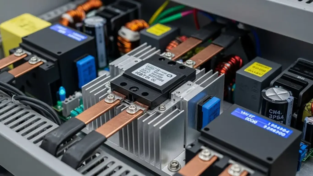
3.3 Drive Loss and Auxiliary Losses
Drive losses include gate charge/discharge losses and static power consumption of drive circuits. The total gate charge (Qg) of SiC MOSFETs is typically 30-50% smaller than same-rated silicon IGBTs, and drive voltage amplitude is smaller (typically -4V/+15V or -5V/+20V), resulting in lower energy requirements per switching cycle. However, because SiC systems often operate at higher switching frequencies, total drive losses may not necessarily decrease, requiring comprehensive trade-offs in system design.
Dead-time losses also affect system efficiency. To avoid shoot-through in bridge arms, dead time must be set between upper and lower arm switching devices. During dead time, current freewheels through body diodes or anti-parallel diodes, generating additional losses. SiC MOSFET body diode characteristics are superior to silicon IGBT freewheeling diodes, and due to fast switching speeds, shorter dead times can be set (100-200ns vs 500-1000ns), thereby reducing dead-time losses.
The loss composition under the condition of 1200 V / 10-20 A
| Loss Component | Si IGBT | SiC MOSFET | Typical Trend |
|---|---|---|---|
| Conduction Loss | Medium | Low | ↓ 20–50% |
| Turn-On Switching Loss (Eon) | High | Very Low | ↓ 60–80% |
| Turn-Off Switching Loss (Eoff) | High | Low | ↓ 50–70% |
| Diode Reverse Recovery Loss | High | Extremely Low | ↓ >80% |
| Total Device Loss | Baseline | Significantly Reduced | ↓ 30–50% (typical) |
IV. System Efficiency Comparison in Typical Application Scenarios
4.1 Electric Vehicle Traction Systems
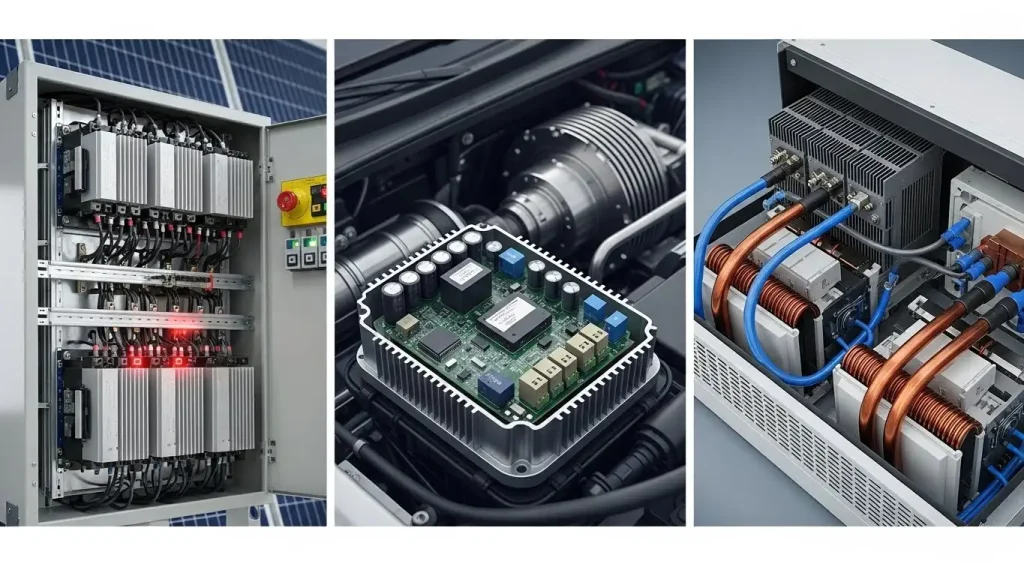
Electric vehicle main drive inverters represent the most representative application scenario for SiC technology. Under WLTC driving cycles, motors frequently operate at partial load conditions, where device light-load efficiency is crucial. Inverters using SiC solutions can achieve 2-4% efficiency improvements in the 10-30% load range and 1-2% efficiency improvements at full load. Comprehensively considering the entire driving cycle, system efficiency improves from 94-95% for traditional silicon solutions to 97-98%.
This efficiency improvement directly translates into increased driving range. For vehicles with 80kWh battery packs, a 2% efficiency improvement equates to approximately 10-15km additional range. Furthermore, due to reduced SiC device losses, heat sink volume can be reduced by 30-40%, total inverter volume reduced by 20-30%, and weight reduced by 15-20%. This is significant for space-constrained vehicle applications and strict lightweighting requirements.
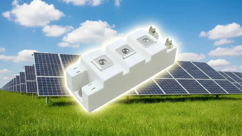
4.2 Photovoltaic Grid-Tied Inverters
Photovoltaic inverters need to maintain high efficiency across wide ranges of input voltage and output power. After adopting SiC devices, inverters can use two-stage topology to replace traditional three-stage topology, eliminating the Boost stage and simplifying system complexity. In CEC weighted efficiency (US standard) or European efficiency (European standard) tests, SiC solutions can achieve peak efficiencies of 98.5-99%, significantly higher than silicon solutions’ 97-98%.
More importantly, SiC inverter efficiency advantages are more pronounced under low-light conditions (10-30% rated power), maintaining efficiencies above 95%, while silicon solutions typically drop to 90-93% under these conditions. Considering that photovoltaic systems operate at medium to low power most of the year, SiC solutions can increase annual energy generation by 1.5-2.5%, which has important implications for large-scale photovoltaic power plant investment returns.
4.3 Data Center Server Power Supplies
Data centers have extremely stringent power efficiency requirements, with 80 PLUS Titanium certification requiring 90-96% efficiency across 20-100% loads. PFC (Power Factor Correction) circuits and LLC resonant converters using SiC devices can operate at higher frequencies (200-500kHz), with magnetic component volumes reduced by over 60%, and power density improved from 20-30 W/in³ for traditional solutions to 50-100 W/in³.
In actual deployments, data center-level efficiency improvements are highly significant. For a 10MW-scale data center, a 1% efficiency improvement means saving hundreds of thousands of dollars in electricity costs annually and reducing corresponding cooling requirements and carbon emissions. Additionally, smaller power module volumes allow servers to accommodate more computing units, improving overall computing capacity.

4.4 Industrial Motor Drives
In industrial inverter applications, SiC solution advantages manifest in wider speed regulation ranges and higher dynamic response speeds. Because switching frequencies can be increased above 50kHz, motor torque ripple is significantly reduced, and noise levels drop by 10-15 dB, which is particularly important for high-precision servo systems and low-noise requirement applications. In terms of system efficiency, rated operating conditions can improve from 92-94% to 95-97%, with considerable energy-saving effects for year-round operation.
For high-power transmission systems (such as fans and pumps), adopting SiC devices enables more refined speed control, achieving additional 5-10% energy savings through optimized operating conditions. Combining device efficiency improvements and system optimization, total energy-saving potential can reach 10-15%.
| Application Fields | GaN | SiC | Efficiency Improvement |
|---|---|---|---|
| Photovoltaic Inverter (50-100 kW) | 97.5-98.2% | 98.5-99.0% | +0.8-1.5% |
| Traction PCS (100-250 kW) | 97-98% | 98.5-99% | +1-2% |
| EV OBC (6-11 kW) | 94-95% | 96-97% | +1.5-2% |
| UPS (Commercial) | 96-97% | 98-99% | +1-2% |
| DC/DC Converter | 95-96% | 97-98% | +1-2% |
V. Summary of SiC Power Module Performance Advantages
Synthesizing the above analysis, the core advantages of SiC power modules can be summarized as follows:
Efficiency Improvement: In typical applications, system efficiency can improve by 2-5 percentage points, with advantages being even more pronounced under partial load conditions. This improvement not only reduces operating costs but also aligns with global energy conservation and emission reduction trends.
Power Density: Due to increased switching frequency and reduced heat generation, passive component and heat sink volumes can be significantly reduced, with system power density improving 2-3 times. This is crucial for space-constrained applications (such as automotive and aerospace).
High-Temperature Capability: Higher junction temperature margins enable systems to operate reliably in harsh environments or allow simplified thermal design at the same ambient temperature, reducing system costs. In some applications, passive cooling can even be achieved, completely eliminating fans and improving reliability.
Dynamic Performance: Faster switching speeds result in better system dynamic response, which is valuable for applications requiring rapid load change response (such as motor drives and grid support).
Reliability Improvement: Lower thermal stress and higher material stability extend module service life and reduce maintenance costs, which is particularly critical for applications requiring 25+ year lifetimes such as wind and solar power.
VI. Engineering Selection Conclusions and Recommendations
In practical engineering applications, selection between SiC and Si power modules requires careful consideration of performance requirements, cost budgets, and technology maturity, among other factors.
Strongly Recommended SiC Scenarios: Electric vehicle main drive inverters, onboard chargers (OBC), high power density photovoltaic inverters (especially string and residential systems), data center high-density power supplies, high-speed motor drives, and aerospace power systems. In these applications, SiC performance advantages can be fully realized, and system-level economics already exceed silicon solutions.
Optional SiC Scenarios: Industrial medium to high power inverters, energy storage converters (PCS), charging stations, UPS power supplies, welding power supplies. In these applications, SiC can bring significant performance improvements, but evaluation based on specific project cost sensitivity is needed. Currently, with rapidly declining SiC device prices, penetration rates in these fields are rapidly increasing.
Postpone SiC Adoption Scenarios: Low-cost home appliance drives, low-power adapters, mature low-frequency (below 10kHz) industrial equipment retrofits. In these applications, performance requirements are relatively low, and cost is the primary consideration. Traditional silicon solutions still offer better cost-performance ratios.
Key Selection Considerations: First, evaluate specific application requirements for efficiency, power density, and operating temperature. Second, consider the impact of production scale on costs (SiC unit costs are more competitive in high-volume applications). Third, evaluate team proficiency with SiC technology, including experience in circuit design, layout, and EMC handling.
From a technology development trend perspective, SiC device costs are declining at 20-30% annually while performance continues to improve. 1200V and 650V voltage class SiC MOSFETs have entered large-scale commercial deployment, and high-voltage SiC devices above 3300V are rapidly maturing. In packaging technology, innovations such as double-sided cooling and embedded packaging further enhance module performance. By 2030, SiC devices are expected to dominate medium to high power (above 10kW) power electronic systems.
For engineers, the current period represents a critical window for learning and mastering SiC technology. It is recommended to include SiC solutions in consideration from the initial design stage of new projects, conducting technology pre-research and small-batch validation. Even if current projects still adopt silicon solutions, interfaces, and space should be reserved for future technology upgrades. Meanwhile, attention must be paid to SiC device specificities, such as gate drive voltage ranges, short-circuit withstand times, and Miller capacitance characteristics, with targeted measures adopted in circuit design and PCB layout.
Conclusion
SiC power modules represent the development direction of power electronics technology. Their comprehensive advantages over traditional silicon-based modules are driving power conversion systems toward higher efficiency, higher power density, and higher reliability. Although current SiC device costs remain higher than silicon devices, from a system-level perspective, comprehensive benefits including efficiency improvements, volume reductions, and thermal simplification, have already demonstrated favorable economics in numerous applications. As the supply chain matures and economies of scale emerge, SiC technology will inevitably play a core role in the future green energy revolution. Engineers should closely track technology development dynamics and introduce SiC solutions at appropriate times to maintain product technical competitiveness and market leadership positions.


