What is Silicon Carbide Complete SiC Technology Guide
Discover what silicon carbide is with this complete SiC technology guide properties manufacturing devices and key power electronics applications
If you’ve been following the surge in electric vehicles and renewable energy systems, you’ve probably heard a lot about Silicon Carbide (SiC)—and for good reason. This wide bandgap semiconductor is transforming power electronics with its unmatched efficiency and thermal performance, leaving traditional silicon devices in the dust.
But what exactly is SiC technology, and why is it becoming the go-to solution for everything from EV inverters to solar power converters? In this complete guide, you’ll get a clear, no-fluff breakdown of Silicon Carbide—from its unique properties and manufacturing processes to real-world applications and future potential. Ready to uncover why SiC is a game-changer in modern electronics? Let’s dive in!
What Is Silicon Carbide (SiC)?
Silicon carbide (SiC) is a wide bandgap semiconductor made from silicon (Si) and carbon (C) with the chemical formula SiC. It combines semiconductor behavior with ceramic‑like strength, which is why it’s now central to next‑generation power electronics.
Chemical Composition and Crystal Structure
At the atomic level, SiC is:
- Composition: One silicon atom bonded to one carbon atom (Si–C)
- Bonding: Strong covalent bonds, giving high hardness and thermal stability
- Crystal structure: Forms in many stacking arrangements called polytypes, all based on tetrahedral Si–C bonding
These crystal structures determine key silicon carbide properties such as bandgap, electron mobility, and breakdown voltage, which directly impact device performance.
Natural Moissanite vs Synthetic Silicon Carbide
In nature, SiC appears as moissanite, an extremely rare mineral found in meteorites and some rocks. It’s:
- Too scarce and impure for electronics
- Mostly known today as a gemstone
Modern silicon carbide used in SiC power electronics is almost entirely synthetic, grown under controlled conditions to achieve:
- High purity for low losses
- Low defect density for high yield and reliability
- Wafer formats compatible with semiconductor lines
Key SiC Polytypes: 4H, 6H, 3C and Why They Matter
SiC is unique because it exists in many polytypes. The most important for electronics are:
4H‑SiC
- Wide bandgap (~3.26 eV)
- High breakdown voltage and good electron mobility
- Industry standard for SiC MOSFETs and SiC Schottky diodes
6H‑SiC
- Slightly different band structure
- Used historically but now less dominant in power devices
3C‑SiC
- Cubic structure (similar to silicon)
- Higher mobility but more crystal defects and growth challenges
These polytypes let us tune performance for high‑voltage, high‑frequency, and high‑temperature applications. For example, 4H‑SiC enables thinner, higher‑voltage devices than silicon, which is critical in EV inverters, onboard chargers, and renewable energy inverters.
Brief History: From Abrasive to Power Electronics
SiC has existed in industry for more than a century, but its role has changed dramatically:
- Late 1800s–early 1900s:
- First synthesized for use as an abrasive and refractory material due to its hardness and heat resistance.
- Mid‑20th century:
- Used in high‑temperature components and early LEDs.
- 1990s–2000s:
- Advances in SiC wafer production, epitaxial growth, and device processing make SiC Schottky diodes and first SiC MOSFETs viable.
- 2010s–today:
- SiC becomes a core technology in power electronics, especially for:
- Electric vehicle inverters and onboard chargers
- Solar and wind power converters
- Fast charging infrastructure and industrial drives
- SiC becomes a core technology in power electronics, especially for:
This shift from a materials commodity to a semiconductor platform is what now allows companies like ours to design high‑performance SiC power modules tailored for global EV, renewable, and industrial markets.
Silicon Carbide Properties: Why SiC Beats Silicon
Silicon carbide (SiC) is a wide bandgap semiconductor, and its physical properties are the main reason it’s taking over next‑gen power electronics.
Wide bandgap and performance
SiC has a bandgap of about 3.2 eV (4H‑SiC) vs 1.12 eV for silicon. That wider bandgap means:
- Much lower leakage current at high temperature
- Higher breakdown voltage at the same chip size
- High‑temperature operation (junction temps >175–200°C are realistic)
In practice, this lets us design smaller, faster, and more efficient SiC MOSFETs and SiC Schottky diodes than possible on silicon.
High thermal conductivity and heat resistance
SiC has thermal conductivity ~3–4.9 W/cm·K, far above silicon (~1.5 W/cm·K). Benefits:
- Better heat spreading inside the die
- Smaller heatsinks and cooling systems
- More power in the same footprint without thermal runaway
This is exactly why SiC shines in EV inverters, onboard chargers, and fast chargers where heat is the main limiter.
High breakdown electric field strength
SiC’s critical electric field is about 10× higher than silicon. For power designers, this means:
- Thinner drift layers for the same voltage rating
- Lower on‑resistance (Rds(on)) at high voltage
- More compact high‑voltage SiC devices (650 V, 1200 V, 1700 V and beyond)
That’s the key to making high‑voltage, fast-switching power devices that still keep conduction and switching losses low.
Mechanical hardness and chemical stability
SiC is extremely hard (close to diamond on the Mohs scale) and chemically robust:
- High wear resistance and surface durability
- Excellent corrosion resistance in harsh industrial environments
- Stable operation in high‑temperature, high‑power systems
This directly supports long‑life systems such as rail traction, wind converters, and industrial motor drives.
Low thermal expansion and strong reliability
SiC has a relatively low coefficient of thermal expansion, which helps:
- Reduce mechanical stress during thermal cycling
- Improve package and solder joint reliability
- Maintain stable performance over long service life
For applications like fast charging, data centers, and high‑reliability power modules, this translates to fewer failures and longer uptime.
SiC vs silicon properties comparison
| Property | Silicon (Si) | Silicon Carbide (SiC, 4H) | Impact on Power Electronics |
|---|---|---|---|
| Bandgap (eV) | ~1.12 | ~3.2 | Higher temp operation, lower leakage |
| Thermal conductivity (W/cm·K) | ~1.5 | ~3–4.9 | Better heat removal, smaller cooling systems |
| Critical electric field (MV/cm) | ~0.3 | ~2.5–3 | Higher breakdown voltage, thinner drift region |
| Max junction temperature (°C) | ~150 | 175–200+ | More robust under overload and harsh environments |
| Electron saturation velocity | Lower | Higher | Faster switching, lower switching loss |
| Thermal expansion (ppm/°C) | Higher | Lower | Improved mechanical reliability over lifetime |
These silicon carbide properties are exactly what we leverage when we design high‑efficiency SiC power modules and diodes, such as our 650 V 4 A SiC Schottky diode, for demanding EV, renewable, and industrial applications.
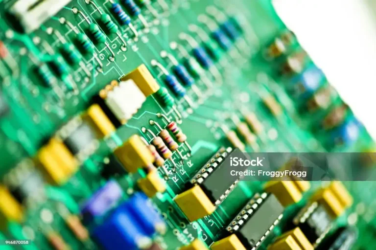
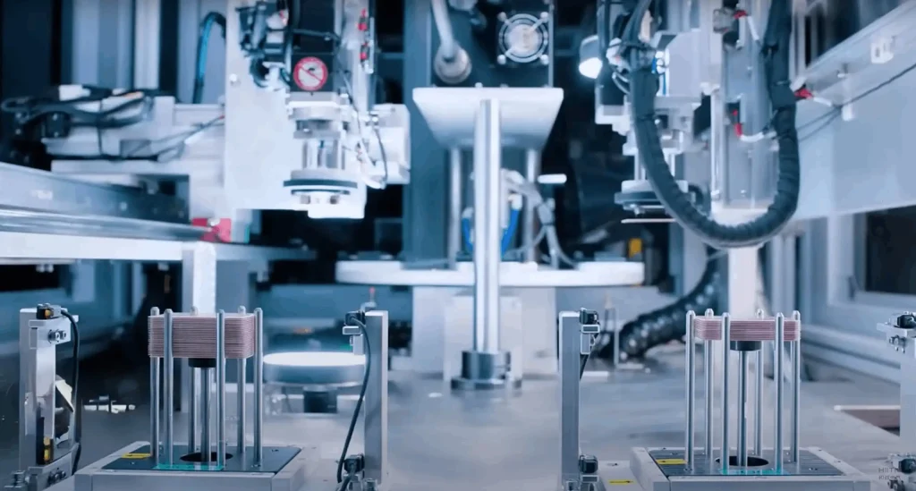
Silicon Carbide Manufacturing Process

Silicon carbide manufacturing is not simple or cheap, but it’s the reason SiC power electronics can beat traditional silicon on efficiency and power density.
Acheson Process: Making Raw SiC
Most SiC starts with the Acheson process:
- Mix silica sand and carbon (usually petroleum coke)
- Heat in a resistance furnace to around 2,000–2,500°C
- Form crude SiC powder, then crush, clean, and sort by grade
This route is great for abrasives and base material, but it’s not pure or controlled enough for high‑end SiC power devices on its own.
Lely Method: Bulk SiC Crystal Growth
For electronics, we need high‑quality single crystals:
- The Lely method (and improved variants) grows bulk SiC crystals in a graphite crucible
- SiC powder sublimates at high temperature and re‑deposits as a single crystal (boule)
- This boule becomes the source for SiC wafer production
Crystal growth is slow, energy‑intensive, and extremely sensitive to defects and contamination.
CVD: High‑Quality SiC Layers
Once we have substrates, we go to chemical vapor deposition (CVD):
- Gas precursors (like silane and hydrocarbons) react at high temperature
- Grow ultra‑pure, controlled SiC epitaxial layers on the wafer
- Fine‑tune thickness, doping, and uniformity for SiC MOSFETs, SiC Schottky diodes, and high‑voltage devices
CVD is the heart of SiC epitaxial growth, and it directly sets breakdown voltage, switching behavior, and leakage performance.
SiC Wafers, Epitaxy, and Wafer Size
From boule to device:
- Slice the crystal into wafers, grind, lap, and polish
- Grow epi layers via CVD for the target device class (650 V, 1200 V, 1700 V, and beyond)
- Process wafers into chips, then assemble into SiC power modules and discrete devices
The industry is shifting hard from 100 mm to 150 mm and 200 mm SiC wafers to cut cost per amp and per kilowatt. Larger wafers mean more dies per run and better economies of scale, especially for high‑current modules that compete with advanced silicon IGBTs like this high‑voltage 3300 V, 1500 A IGBT power module.
Manufacturing Challenges and Yield Issues
SiC manufacturing is still tougher than silicon:
- Crystal defects (micropipes, dislocations) hit yield and limit breakdown voltage
- Larger wafers are harder to keep uniform in epi thickness and doping
- Wafer bow, stress, and surface defects impact lithography and reliability
- Tooling, consumables, and process windows are tighter and more expensive than for silicon
As we push to higher voltages and currents, the bar for wafer quality keeps rising. That’s exactly why we focus on tightly controlled supply chains and process control—device cost, performance, and reliability all start at the SiC wafer and epitaxy level.
Contact HIITIO for Your Custom Solution
Advantages of SiC Technology Over Silicon
Silicon carbide (SiC) changes the game for power electronics. Compared with traditional silicon, SiC devices deliver higher efficiency, smaller systems, and better reliability, especially in demanding environments like EVs, renewables, and industrial drives.
Higher efficiency & lower conduction losses
SiC MOSFETs and SiC Schottky diodes have:
- Much lower switching and conduction losses at high voltage
- Stable performance at high temperature, so you stay efficient even under heavy load
- Higher breakdown voltage, which lets you design compact high‑voltage stages without wasting power
In real EV inverters or solar inverters, that directly turns into lower energy loss, cooler operation, and higher system efficiency.
Faster switching & high‑frequency operation
As a wide bandgap semiconductor, SiC supports:
- Faster switching speeds than silicon IGBTs and MOSFETs
- Higher switching frequencies, reducing passive component size
- Cleaner waveforms, with lower switching loss and improved power density
This is why SiC power modules are now standard in fast, high‑power converters and DC‑DC stages.
Better thermal management & smaller heatsinks
Key silicon carbide properties like high thermal conductivity and high temperature capability mean:
- Less heat per watt of power handled
- Higher junction temperatures allowed safely
- Smaller heatsinks and cooling systems without compromising reliability
In practice, a SiC‑based design can shrink the whole thermal stack while still running cooler than a silicon design at the same power level.
Smaller, lighter power system design
Because SiC enables high‑frequency, high‑efficiency operation, you can:
- Use smaller inductors, transformers, and capacitors
- Cut overall weight and volume of inverters, onboard chargers, and motor drives
- Increase power density without needing exotic cooling
For OEMs, that means more power in the same footprint—or the same power in a smaller box.
Improved reliability in harsh environments
SiC is built for tough conditions:
- High temperature tolerance and low thermal expansion improve long‑term reliability
- Excellent chemical and mechanical stability helps in rail, aerospace, and industrial environments
- High breakdown voltage and robust die design make SiC ideal for high‑voltage, high‑stress systems
This is especially valuable in EV drivetrains, wind turbines, and heavy industrial motor drives where uptime is critical.
System‑level benefits in real applications
When you step back and look at the system, SiC technology delivers:
- Lower total system cost at the same performance level, thanks to reduced cooling and magnetics
- Higher efficiency in EV inverters, onboard chargers, and renewable energy inverters
- More compact, lighter power modules for easier integration and higher power density
For example, our high‑current 1200 V SiC power module solutions are designed to give OEMs a direct path to smaller, more efficient inverters and converters without sacrificing robustness at high voltage and high temperature.
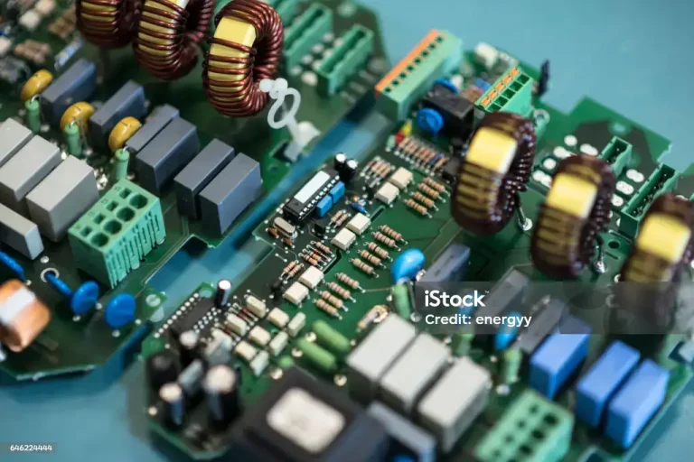
SiC Power Devices and Components
Silicon carbide power devices sit at the core of modern high‑efficiency power electronics. By combining a wide bandgap, high thermal conductivity, and high breakdown voltage, SiC components deliver higher power density, lower losses, and better reliability than traditional silicon devices.
SiC Schottky Barrier Diodes (SBDs)
SiC Schottky diodes are now the default choice for high‑efficiency power conversion:
- Ultra‑fast switching with virtually no reverse recovery loss
- Low forward voltage drop, cutting conduction losses and heat
- Ideal for PFC stages, DC‑DC converters, EV onboard chargers, and solar inverters
- Stable performance at high temperatures and high voltage
In real systems, swapping silicon diodes for SiC SBDs directly boosts efficiency and allows smaller magnetics and heatsinks.
SiC MOSFETs and Discrete Devices
SiC MOSFETs are the main SiC power switches used today:
- High breakdown voltage (typically 650 V–1700 V and beyond)
- Low Rds(on) and low switching losses, even at high temperature
- Enables high‑frequency, high‑efficiency designs in EV inverters, motor drives, and fast chargers
- Smaller, lighter systems with higher power density
For example, a 1200 V SiC MOSFET in TO‑247 package can replace multiple parallel silicon devices, simplifying design and boosting efficiency in chargers, UPS, and industrial power supplies. HIITIO’s own 1200 V 40 mΩ silicon carbide power MOSFET in TO‑247‑3L is built specifically around this need for low loss and robust switching in global EV and renewable applications.
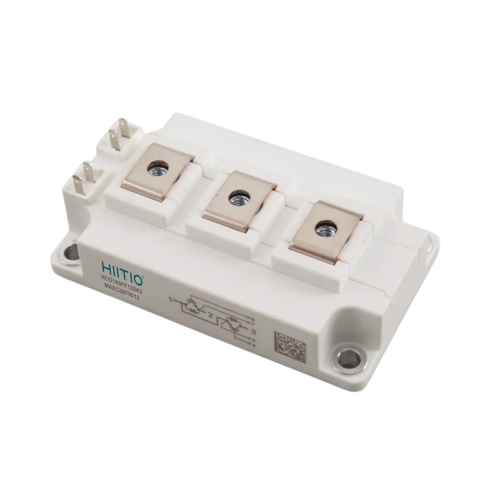
SiC Power Modules and Integrated Solutions
When power levels go up, SiC power modules unlock the real value of SiC technology:
- Multiple SiC MOSFETs and diodes integrated in one package
- Lower stray inductance, optimized layouts, and better thermal paths
- Perfect for EV traction inverters, wind and solar converters, industrial drives, and high‑power chargers
- Supports compact, high‑efficiency, high‑reliability systems
As a China‑based manufacturer focused on the global market, we design SiC power modules to drop into standard footprints, so OEMs can scale power and efficiency without re‑inventing their entire platform.
Emerging SiC JFETs and Hybrid IGBT Structures
Beyond MOSFETs and diodes, the SiC ecosystem is expanding:
- SiC JFETs offer normally‑on behavior with very low conduction losses, useful in niche high‑efficiency designs.
- Hybrid IGBT + SiC diode or SiC MOSFET structures combine the ruggedness and cost familiarity of IGBTs with the speed and efficiency of SiC, easing migration from pure silicon to wide bandgap technology.
These hybrid architectures are especially attractive in applications like rail, heavy industrial drives, and cost‑sensitive high‑power converters where full SiC is not yet mandatory.
How HIITIO Designs High‑Performance SiC Power Modules
At HIITIO, we design SiC modules for real‑world use, not lab demos. Our approach focuses on:
- Application‑driven design – optimized topologies for EV inverters, chargers, solar/wind inverters, and motor drives
- Low‑loss layouts – minimized inductance, carefully tuned parasitics for stable, ultra‑fast switching
- Advanced packaging – high‑performance substrates, copper bond, and thermal paths to exploit SiC’s heat capability
- Easy integration – gate‑drive compatibility, standard footprints, and robust short‑circuit and surge behavior
- Global reliability standards – tested to meet strict requirements across Europe, North America, and Asia markets
By combining our SiC MOSFETs and diodes into optimized power modules, we give system designers a straightforward way to upgrade from silicon to high‑efficiency SiC power electronics with measurable gains in efficiency, size, and lifetime.
Silicon Carbide Applications in Real Power Systems
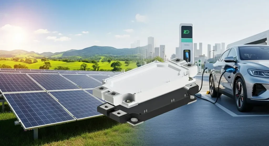
Electric vehicles: inverters, onboard chargers, DC‑DC converters
In EVs, silicon carbide (SiC) is now the go‑to wide bandgap semiconductor for high‑efficiency power stages:
- Traction inverters: SiC MOSFETs cut conduction and switching losses, boost driving range, and shrink the cooling system.
- Onboard chargers (OBC): SiC lets you build compact, high‑power OBCs (11–22 kW) that run cooler and charge faster.
- DC‑DC converters: High‑frequency SiC designs reduce magnetics size and help stabilize the 12 V / 48 V bus under harsh conditions.
Renewable energy: solar and wind inverters
SiC power electronics are a perfect fit for solar and wind systems that run all day, every day:
- Solar inverters using SiC Schottky diodes and MOSFETs hit higher efficiency at both full and partial load.
- Wind converters benefit from higher voltage capability and better thermal performance, which directly improves uptime and energy yield.
Industrial motor drives and power supplies
For industrial users, SiC is about reliability and size:
- Drives for pumps, compressors, and factory automation run cooler and handle wider input voltages.
- High‑power SMPS and UPS systems use SiC to reach higher power density and lower total cost of ownership over the life of the system.
Rail, aerospace, and high‑reliability systems
In rail traction, aviation power units, and other mission‑critical systems, SiC’s high temperature capability and high breakdown voltage are key:
- Lighter converters and inverters with higher efficiency
- Better performance in vibration, altitude, and extreme temperature environments
Charging infrastructure and fast chargers
DC fast chargers are pushing 350 kW and beyond. SiC makes that practical:
- Higher switching frequency reduces filter and transformer size
- Higher efficiency lowers operating costs and eases cooling at charging sites
Where needed, SiC diodes can also be paired with robust IGBT stages, as in a 62mm, 1200 V high‑current power module similar to this 1200 V 450 A IGBT power module, to balance cost and performance.
Data centers and high‑voltage grid applications
From server power to transmission‑level gear, SiC is becoming a core technology:
- Data centers: Front‑end PFC and DC‑DC stages using SiC cut energy loss and free up power budget for IT load.
- Grid and HVDC: High‑voltage SiC devices improve efficiency and enable more compact substation and converter designs.
Across all of these, the main value of silicon carbide technology is simple: more power, less loss, smaller systems, and higher reliability.
Challenges and Limitations of SiC Technology

Silicon carbide is powerful, but it’s not plug‑and‑play. If you’re moving from silicon to SiC, these are the real‑world roadblocks you’ll run into and what ongoing R&D is doing to fix them.
Higher device and module cost vs silicon
SiC devices and SiC power modules are still more expensive than standard silicon IGBTs or MOSFETs. The reasons are clear:
- More complex SiC wafer production and crystal growth
- Lower manufacturing yield
- Limited supply chain compared with silicon
That said, at the system level, SiC often wins:
- Smaller magnetics and filters
- Reduced cooling (heatsinks, fans, liquid loops)
- Higher efficiency, especially in EV inverters, fast chargers, and renewable energy inverters
In most high‑power, high‑efficiency designs, total cost of ownership is already shifting in favor of SiC.
Crystal defects, wafer quality, and yield
SiC is hard to grow. Defects like micropipes, dislocations, and stacking faults can:
- Lower breakdown voltage and reliability
- Reduce usable wafer area
- Push up device cost
Ongoing SiC epitaxial growth R&D focuses on:
- Reducing defect density on 150 mm and 200 mm SiC wafers
- Improving uniformity of doping and thickness
- Tightening process control for higher yield
Every step forward in wafer quality directly cuts device cost and improves long‑term reliability.
Packaging, gate‑drive, and design complexity
SiC is a fast switching power device with very high dv/dt and di/dt. That brings new design challenges:
- Stray inductance is deadly for overshoot and EMI
- Gate‑drive design must handle higher dv/dt, negative voltage swings, and precise gate resistance
- Layout and packaging need to be optimized for low parasitics and good thermal paths
Modern SiC power modules, such as advanced 2200 V / 450 A SiC solutions in compact module packages, use low‑inductance layouts and high‑performance substrates to manage this. With a solid reference design and proper gate‑drive strategy, SiC complexity becomes manageable.
Supply chain capacity and availability
Demand for SiC power electronics in EVs, charging infrastructure, solar inverters, and industrial drives is growing faster than capacity:
- Long lead times on wafers and devices
- Limited number of high‑volume, high‑quality suppliers
- Geographical concentration of key wafer and epi players
This is improving as more fabs expand SiC lines, new 200 mm SiC wafer capacity comes online, and more ecosystem players enter the market, but supply planning is still critical for large programs.
How ongoing R&D is reducing these barriers
The gap between Si and SiC is closing fast. R&D is attacking all the pain points:
- Cost: Larger wafers, better yield, and optimized process flows
- Quality: Lower defect density, improved epitaxy, and tighter control of SiC bandgap and doping profiles
- Design: Better gate‑driver ICs, reference designs, and more robust packaging for high‑temperature semiconductors
- Reliability: Long‑term testing in EV inverters, solar inverter SiC platforms, and high‑voltage grid systems
For designers targeting high efficiency, high power density, and harsh environments, the current challenges of SiC are real—but shrinking fast.
Future of Silicon Carbide Technology
Market growth and adoption trends
Silicon carbide technology is moving from “early adoption” to “mainstream”. Driven by EVs, renewables, and high‑efficiency power supplies, the SiC market is growing at a double‑digit annual rate. OEMs in Europe, North America, and Asia are locking in long‑term SiC supply to secure 1200V and 1700V platforms for inverters, onboard chargers, and DC‑DC converters. As 200mm SiC wafers scale up and yields improve, we’re going to see SiC power devices replace silicon in more high‑power, high‑temperature applications.
Next‑gen SiC device architectures
The next wave of wide bandgap semiconductor design is all about higher efficiency at higher voltage and current:
- Advanced SiC MOSFET structures with lower Rds(on) and reduced switching losses
- Optimized SiC Schottky diodes for ultra‑fast, low‑loss freewheeling and PFC stages
- High‑current SiC power modules, like our 62mm 1200V SiC module, targeting compact, high‑density converters
- Co‑pack solutions and hybrid topologies that mix SiC, IGBT, and fast diodes for cost‑optimized designs
These architectures push higher switching frequencies, smaller magnetics, and tighter system integration.
Integration with Si, GaN, and other wide bandgap tech
SiC won’t replace everything; it will sit alongside silicon and GaN:
- SiC: best for high voltage, high power (600V–3.3kV+), harsh environments
- GaN: strong in lower‑voltage, very high‑frequency consumer and server power
- Silicon: still cost‑effective for low‑end, low‑stress applications
System designers increasingly combine SiC modules on the high‑voltage side with GaN or silicon on the low‑voltage side to hit the best balance of efficiency, cost, and footprint.
Role of SiC in EVs and clean energy transition
Silicon carbide is becoming the default choice for:
- EV inverters – higher efficiency and higher switching speed mean more range and smaller cooling systems
- EV onboard chargers and DC‑DC converters – SiC cuts losses and enables higher power in the same or smaller package
- Solar and wind inverters – higher efficiency, higher power density, and better reliability in outdoor and high‑temperature environments
By reducing energy losses across the whole power chain, SiC directly supports CO₂ reduction targets and the global clean energy transition.
How HIITIO pushes SiC performance and cost down
As a leading SiC power module manufacturer in China, I focus on three things:
- High‑performance module design – low‑inductance layouts, optimized thermal paths, and rugged packaging for EV, industrial, and renewable applications
- Cost per kW, not just cost per device – our ED3S 1200V 400A SiC power module delivers high current in a compact footprint, cutting system‑level BOM, cooling, and size
- Manufacturing scale and reliability – tight process control, higher wafer sizes, and continuous R&D to boost yield and consistency
The future of silicon carbide technology is clear: higher power density, wider adoption, and lower $/kW, with manufacturers like HIITIO leading the charge on real‑world, production‑ready SiC power electronics.